Thursday, 30 June 2016

A little spark for sharper sight

A little spark for sharper sight


Brain stimulation temporarily improves visual acuity, according to new research.

Stimulating the visual cortex of the brain for 20 minutes with a mild electrical current can improve vision for about two hours, and those with worse vision see the most improvement, according to a Vanderbilt University study published this week in Current Biology.
"It's actually a very simple idea," said co-author Geoff Woodman, associate professor of psychology. "This kind of stimulation can improve cognitive processing in other brain areas, so if we stimulate the visual system, could we improve processing? Could we make someone's vision better -- not at the level of the eye, like Lasik or glasses, but directly at the level of the brain?"
Twenty young, healthy subjects with normal or near-normal vision were asked to evaluate the relative position of two identical vertical lines and judged whether they were perfectly aligned or offset. The test is more sensitive than a standard eye chart, and gave the researchers are very precise measurement of each subjects' visual acuity.
The researchers then passed a very mild electric current through the area at the back of the brain that processes visual information. After 20 minutes, the subjects were asked to perform the test again, and about 75 percent showed measurable improvement following the brain stimulation.
The researchers performed several variations of this experiment to test the effects of different intensity levels, current directions and electrode placements. This third experiment was important because it confirmed that the electrodes had to be positioned specifically over the brain's visual processing center in order to affect the subjects' eyesight -- that the effect wasn't simply a response to stimulus anywhere in the brain.
They also measured how the stimulus changed the speed with which the brain processed visual information and whether the stimulation also improved the subjects' contrast sensitivity -- their ability to differentiate between multiple shades of gray.
The contrast experiment was notable because they found that the stimulation only improved contrast sensitivity at frequencies also associated with visual acuity, indicating that it was just the subjects' visual acuity that was being affected, not the contrast sensitivity.
Lead author Robert Reinhart, an incoming assistant professor in the Department of Psychological and Brain Sciences at Boston University who conducted this research as a Ph.D. student at Vanderbilt, said this finding had interesting implications for future basic science. "Now we have a new tool that could be valuable for researchers investigating fundamental questions about how the visual system works," he said.
For their last experiment, the researchers wanted to see if the improvement they saw in the first experiment was significant enough to translate into a real-world task -- reading a standard eye chart.
They found that the stimulation effects improved the subjects' vision by an average of 1 to 2 letters, though Reinhart noted that there was significant variation between subjects. "We saw that those who came in with poorer vision, who might be on their way to needing glasses, had these big leaps, while others who came in with excellent vision showed no change."
Reinhart speculated that these findings could be explained in several different ways. The prevailing belief is that the current might simply be boosting the visual signals so certain neurons can process them more rapidly, but Reinhart thinks it's also possible that the current essentially injects white noise into the visual system, which drowns out extraneous information and enables the brain to capture visual information more easily.
The researchers stress that much more research needs to happen in a clinical setting in order to confirm the safety of the procedure and that members of the public should never attempt to replicate the experiment at home.

Story Source:
The above post is reprinted from materials provided by Vanderbilt University. The original item was written by Liz Entman. Note: Materials may be edited for content and length.

Journal Reference:
  1. Robert M.g. Reinhart, Wenxi Xiao, Laura J. Mcclenahan, Geoffrey F. Woodman. Electrical Stimulation of Visual Cortex Can Immediately Improve Spatial VisionCurrent Biology, June 2016 DOI:10.1016/j.cub.2016.05.019

Cite This Page:

Vanderbilt University. "A little spark for sharper sight." ScienceDaily. ScienceDaily, 30 June 2016. <www.sciencedaily.com/releases/2016/06/160630140900.htm>.
Wednesday, 29 June 2016

New Hydrogel Hybrid Could Be Used To Make Artificial Skin

New Hydrogel Hybrid Could Be Used To Make Artificial Skin

MIT Develops Tough Hydrogel Hybrid
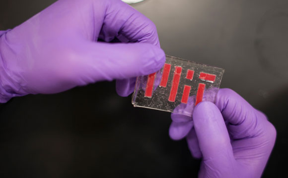
MIT engineers have developed a method to bind gelatin-like polymer materials called hydrogels and elastomers, which could be used to make artificial skin and longer-lasting contact lenses.
If you leave a cube of Jell-O on the kitchen counter, eventually its water will evaporate, leaving behind a shrunken, hardened mass — hardly an appetizing confection. The same is true for hydrogels. Made mostly of water, these gelatin-like polymer materials are stretchy and absorbent until they inevitably dry out.
Now engineers at MIT have found a way to prevent hydrogels from dehydrating, with a technique that could lead to longer-lasting contact lenses, stretchy microfluidic devices, flexible bioelectronics, and even artificial skin.
See how MIT researchers designed a hydrogel that doesn’t dry out. Video: Melanie Gonick/MIT

The engineers, led by Xuanhe Zhao, the Robert N. Noyce Career Development Associate Professor in MIT’s Department of Mechanical Engineering, devised a method to robustly bind hydrogels to elastomers — elastic polymers such as rubber and silicone that are stretchy like hydrogels yet impervious to water. They found that coating hydrogels with a thin elastomer layer provided a water-trapping barrier that kept the hydrogel moist, flexible, and robust. The results are published in the journal Nature Communications.
Zhao says the group took inspiration for its design from human skin, which is composed of an outer epidermis layer bonded to an underlying dermis layer. The epidermis acts as a shield, protecting the dermis and its network of nerves and capillaries, as well as the rest of the body’s muscles and organs, from drying out.
The team’s hydrogel-elastomer hybrid is similar in design to, and in fact multiple times tougher than, the bond between the epidermis and dermis. The team developed a physical model to quantitatively guide the design of various hydrogel-elastomer bonds. In addition, the researchers are exploring various applications for the hybrid material, including artificial skin. In the same paper, they report inventing a technique to pattern tiny channels into the hybrid material, similar to blood vessels. They have also embedded complex ionic circuits in the material to mimic nerve networks.
“We hope this work will pave the way to synthetic skin, or even robots with very soft, flexible skin with biological functions,” Zhao says.
The paper’s lead author is MIT graduate student Hyunwoo Yuk. Co-authors include MIT graduate students German Alberto Parada and Xinyue Liu and former Zhao group postdoc Teng Zhang, now an assistant professor at Syracuse University.
MIT Develops Tough New Hydrogel Hybrid
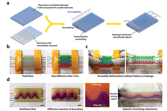
Figure (a) shows the fabrication procedure for a hydrogel-elastomer microfluidic chip. Figure (b) shows that the hydrogel-elastomer microfluidic hybrid supports convection of chemicals (represented by food dye in different colors) in the microfluidic channels and diffusion of chemicals in the hydrogel, even when the material is stretched, as seen in figure (c). In figure (d), the microfluidic hybrid is used as a platform for a diffusion-reaction study. Acid and base solutions from two microfluidic channels diffuse in the pH-sensitive hydrogel and form regions of different colors (light red for acid and dark violet for base).
Getting under the skin
In December 2015, Zhao’s team reported that they had developed a technique to achieve extremely robust bonding of hydrogels to solid surfaces such as metal, ceramic, and glass. The researchers used the technique to embed electronic sensors within hydrogels to create a “smart” bandage. They found, however, that the hydrogel would eventually dry out, losing its flexibility.
Others have tried to treat hydrogels with salts to prevent dehydration, which Zhao says is effective, but this method can make a hydrogel incompatible with biological tissues. Instead, the researchers, inspired by skin, reasoned that coating hydrogels with a material that was similarly stretchy but also water-resistant would be a better strategy for preventing dehydration. They soon landed on elastomers as the ideal coating, though the rubbery material came with one major challenge: It was inherently resistant to bonding with hydrogels.
“Most elastomers are hydrophobic, meaning they do not like water,” Yuk says. “But hydrogels are a modified version of water. So these materials don’t like each other much and usually can’t form good adhesion.”
The team tried to bond the materials together using the technique they developed for solid surfaces, but with elastomers, Yuk says, the hydrogel bonding was “horribly weak.” After searching through the literature on chemical bonding agents, the researchers found a candidate compound that might bring hydrogels and elastomers together: benzophenone, which is activated via ultraviolet (UV) light.
After dipping a thin sheet of elastomer into a solution of benzophenone, the researchers wrapped the treated elastomer around a sheet of hydrogel and exposed the hybrid to UV light. They found that after 48 hours in a dry laboratory environment, the weight of the hybrid material did not change, indicating that the hydrogel retained most of its moisture. They also measured the force required to peel the two materials apart, and found that to separate them required 1,000 joules per square meters — much higher than the force needed to peel the skin’s epidermis from the dermis.
“This is tougher even than skin,” Zhao says. “We can also stretch the material to seven times its original length, and the bond still holds.”
Expanding the hydrogel toolset
Taking the comparison with skin a step further, the team devised a method to etch tiny channels within the hydrogel-elastomer hybrid to simulate a simple network of blood vessels. They first cured a common elastomer onto a silicon wafer mold with a simple three-channel pattern, etching the pattern onto the elastomer using soft lithography. They then dipped the patterned elastomer in benzophenone, laid a sheet of hydrogel over the elastomer, and exposed both layers to ultraviolet light. In experiments, the researchers were able to flow red, blue, and green food coloring through each channel in the hybrid material.
Yuk says in the future, the hybrid-elastomer material may be used as a stretchy microfluidic bandage, to deliver drugs directly through the skin.
“We showed that we can use this as a stretchable microfluidic circuit,” Yuk says. “In the human body, things are moving, bending, and deforming. Here, we can perhaps do microfluidics and see how [the device] behaves in a moving part of the body.”
The researchers also explored the hybrid material’s potential as a complex ionic circuit. A neural network is such a circuit; nerves in the skin send ions back and forth to signal sensations such as heat and pain. Zhao says hydrogels, being mostly composed of water, are natural conductors through which ions can flow. The addition of an elastomer layer, he says, acts as an insulator, preventing ions from escaping — an essential combination for any circuit.
To make it conductive to ions, the researchers submerged the hybrid material in a concentrated solution of sodium chloride, then connected the material to an LED light. By placing electrodes at either end of the material, they were able to generate an ionic current that switched on the light.
“We show very beautiful circuits not made of metal, but of hydrogels, simulating the function of neurons,” Yuk says. “We can stretch them, and they still maintain connectivity and function.”
Syun-Hyun Yun, an associate professor at Harvard Medical School and Massachusetts General Hospital, says that hydrogels and elastomers have distinct physical and chemical properties that, when combined, may lead to new applications.
“It is a thought-provoking work,” says Yun, who was not involved in the research. “Among many [applications], I can imagine smart artificial skins that are implanted and provide a window to interact with the body for monitoring health, sensing pathogens, and delivering drugs.”
Next, the group hopes to further test the hybrid material’s potential in a number of applications, including wearable electronics and on-demand drug-delivering bandages, as well as nondrying, circuit-embedded contact lenses.
“Ultimately, we’re trying to expand the argument of using hydrogels as an advanced engineering toolset,” Zhao says.
This research was funded, in part, by the Office of Naval Research, Draper Laboratory, MIT Institute for Soldier Nanotechnologies, and National Science Foundation.
Publication: Hyunwoo Yuk, et al., “Skin-inspired hydrogel–elastomer hybrids with robust interfaces and functional microstructures,” Nature Communications 7, Article number: 12028 doi:10.1038/ncomms12028
Source: Jennifer Chu, MIT News

Monday, 27 June 2016

New, better way to build circuits for world's first useful quantum computers

New, better way to build circuits for world's first useful quantum computers


The research team led by David Weiss at Penn State University performed a specific single quantum operation on individual atoms in a P-S-U pattern on three separate planes stacked within a cube-shaped arrangement. The team then used light beams to selectively sweep away all the atoms that were not targeted for that operation. The scientists then made pictures of the results by successively focusing on each of the planes in the cube. The photos, which are the sum of 20 implementations of this process, show bright spots where the atoms are in focus, and fuzzy spots if they are out of focus in an adjacent plane -- as is the case for all the light in the two empty planes. The photos also show both the success of the technique and the comparatively small number of targeting errors.

The era of quantum computers is one step closer as a result of research published in the current issue of the journalScience. The research team has devised and demonstrated a new way to pack a lot more quantum computing power into a much smaller space and with much greater control than ever before. The research advance, using a 3-dimensional array of atoms in quantum states called quantum bits -- or qubits -- was made by David S. Weiss, professor of physics at Penn State University, and three students on his lab team. He said "Our result is one of the many important developments that still are needed on the way to achieving quantum computers that will be useful for doing computations that are impossible to do today, with applications in cryptography for electronic data security and other computing-intensive fields."
The new technique uses both laser light and microwaves to precisely control the switching of selected individual qubits from one quantum state to another without altering the states of the other atoms in the cubic array. The new technique demonstrates the potential use of atoms as the building blocks of circuits in future quantum computers.
The scientists invented an innovative way to arrange and precisely control the qubits, which are necessary for doing calculations in a quantum computer. "Our paper demonstrates that this novel approach is a precise, accurate, and efficient way to control large ensembles of qubits for quantum computing," Weiss said.
The paper in Science describes the new technique, which Weiss's team plans to continue developing further. The achievement also is expected to be useful to scientists pursuing other approaches to building a quantum computer, including those based on other atoms, on ions, or on atom-like systems in 1 or 2 dimensions. "If this technique is adopted in those other geometries, they would also get this robustness," Weiss said.
To corral their quantum atoms into an orderly 3-D pattern for their experiments, the team constructed a lattice made by beams of light to trap and hold the atoms in a cubic arrangement of five stacked planes -- like a sandwich made with five slices of bread -- each with room for 25 equally spaced atoms. The arrangement forms a cube with an orderly pattern of individual locations for 125 atoms. The scientists filled some of the possible locations with qubits consisting of neutral cesium atoms -- those without a positive or a negative charge. Unlike the bits in a classical computer, which typically are either zeros or ones, each of the qubits in the Weiss team's experiment has the difficult-to-imagine ability to be in more than one state at the same time -- a central feature of quantum mechanics called quantum superposition.
Weiss and his team then use another kind of light tool -- crossed beams of laser light -- to target individual atoms in the lattice. The focus of these two laser beams, called "addressing" beams, on a targeted atom shifts some of that atom's energy levels by about twice as much as it does for those of any of the other atoms in the array, including those that were in the path of one of the addressing beams on its way to the target. When the scientists then bathe the whole array with a uniform wash of microwaves, the state of the atom with the shifted energy levels is changed, while the states of all the other atoms are not.
"We have set more qubits into different, precise quantum superpositions at the same time than in any previous experimental system," Weiss said. The scientists also designed their system to be very insensitive to the exact details of the alignments or the power of those light beams they use -- which Weiss said is a good thing because "you don't want to be dependent upon exactly what the intensity of the light is or exactly what the alignment is."
One of the ways that the scientists demonstrated their ability to change the quantum state of individual atoms was by changing the states of selected atoms in three of the stacked planes within the cubic array in order to draw the letters P, S, and U -- the letters that represent Penn State University. "We changed the quantum superposition of the PSU atoms to be different from the quantum superposition of the other atoms in the array," Weiss said. "We have a pretty high-fidelity system. We can do targeted selections with a reliability of about 99.7%, and we have a plan for making that more like 99.99%."
Among the goals that Weiss has for his team's future research is to get the qubits to "have entangled quantum wave functions where the state of one particle is implicitly correlated with the state of the other particles around it." Weiss said that this entangled connection between qubits is a critical element needed for quantum computing. He said he hopes that building on the techniques demonstrated in his team's prototype system eventually will enable his lab to demonstrate high-quality entangling operations for quantum computing. "Filling the cube with exactly one atom per site and setting up entanglements between atoms at any of the sites that we choose are among our nearer-term research goals," Weiss said.

Story Source:
The above post is reprinted from materials provided by Penn State. The original item was written by Barbara K. Kennedy. Note: Materials may be edited for content and length.

Journal Reference:
  1. Y. Wang, A. Kumar, T.-Y. Wu, D. S. Weiss. Single-qubit gates based on targeted phase shifts in a 3D neutral atom arrayScience, 2016; 352 (6293): 1562 DOI: 10.1126/science.aaf2581

Cite This Page:
Penn State. "New, better way to build circuits for world's first useful quantum computers." ScienceDaily. ScienceDaily, 27 June 2016. <www.sciencedaily.com/releases/2016/06/160627132809.htm>

.

Saturday, 25 June 2016

Nanoscientists develop the 'ultimate discovery tool'

Nanoscientists develop the 'ultimate discovery tool'

Rapid discovery power is similar to what gene chips offer biology


A combinatorial library of polyelemental nanoparticles was developed using Dip-Pen Nanolithography. This novel nanoparticle library opens up a new field of nanocombinatorics for rapid screening of nanomaterials for a multitude of properties.

The discovery power of the gene chip is coming to nanotechnology. A Northwestern University research team is developing a tool to rapidly test millions and perhaps even billions or more different nanoparticles at one time to zero in on the best particle for a specific use.
When materials are miniaturized, their properties -- optical, structural, electrical, mechanical and chemical -- change, offering new possibilities. But determining what nanoparticle size and composition are best for a given application, such as catalysts, biodiagnostic labels, pharmaceuticals and electronic devices, is a daunting task.
"As scientists, we've only just begun to investigate what materials can be made on the nanoscale," said Northwestern's Chad A. Mirkin, a world leader in nanotechnology research and its application, who led the study. "Screening a million potentially useful nanoparticles, for example, could take several lifetimes. Once optimized, our tool will enable researchers to pick the winner much faster than conventional methods. We have the ultimate discovery tool."
Using a Northwestern technique that deposits materials on a surface, Mirkin and his team figured out how to make combinatorial libraries of nanoparticles in a very controlled way. (A combinatorial library is a collection of systematically varied structures encoded at specific sites on a surface.) Their study will be published June 24 by the journal Science.
The nanoparticle libraries are much like a gene chip, Mirkin says, where thousands of different spots of DNA are used to identify the presence of a disease or toxin. Thousands of reactions can be done simultaneously, providing results in just a few hours. Similarly, Mirkin and his team's libraries will enable scientists to rapidly make and screen millions to billions of nanoparticles of different compositions and sizes for desirable physical and chemical properties.
"The ability to make libraries of nanoparticles will open a new field of nanocombinatorics, where size -- on a scale that matters -- and composition become tunable parameters," Mirkin said. "This is a powerful approach to discovery science."
Mirkin is the George B. Rathmann Professor of Chemistry in the Weinberg College of Arts and Sciences and founding director of Northwestern's International Institute for Nanotechnology.
"I liken our combinatorial nanopatterning approach to providing a broad palette of bold colors to an artist who previously had been working with a handful of dull and pale black, white and grey pastels," said co-author Vinayak P. Dravid, the Abraham Harris Professor of Materials Science and Engineering in the McCormick School of Engineering.
Using five metallic elements -- gold, silver, cobalt, copper and nickel -- Mirkin and his team developed an array of unique structures by varying every elemental combination. In previous work, the researchers had shown that particle diameter also can be varied deliberately on the 1- to 100-nanometer length scale.
Some of the compositions can be found in nature, but more than half of them have never existed before on Earth. And when pictured using high-powered imaging techniques, the nanoparticles appear like an array of colorful Easter eggs, each compositional element contributing to the palette.
To build the combinatorial libraries, Mirkin and his team used Dip-Pen Nanolithography, a technique developed at Northwestern in 1999, to deposit onto a surface individual polymer "dots," each loaded with different metal salts of interest. The researchers then heated the polymer dots, reducing the salts to metal atoms and forming a single nanoparticle. The size of the polymer dot can be varied to change the size of the final nanoparticle.
This control of both size and composition of nanoparticles is very important, Mirkin stressed. Having demonstrated control, the researchers used the tool to systematically generate a library of 31 nanostructures using the five different metals.
To help analyze the complex elemental compositions and size/shape of the nanoparticles down to the sub-nanometer scale, the team turned to Dravid, Mirkin's longtime friend and collaborator. Dravid, founding director of Northwestern's NUANCE Center, contributed his expertise and the advanced electron microscopes of NUANCE to spatially map the compositional trajectories of the combinatorial nanoparticles.
Now, scientists can begin to study these nanoparticles as well as build other useful combinatorial libraries consisting of billions of structures that subtly differ in size and composition. These structures may become the next materials that power fuel cells, efficiently harvest solar energy and convert it into useful fuels, and catalyze reactions that take low-value feedstocks from the petroleum industry and turn them into high-value products useful in the chemical and pharmaceutical industries.

Story Source:
The above post is reprinted from materials provided by Northwestern University. The original item was written by Megan Fellman. Note: Materials may be edited for content and length.

Journal Reference:
  1. Peng-Cheng Chen, Xiaolong Liu, James L. Hedrick, Zhuang Xie, Shunzhi Wang, Qing-Yuan Lin, Mark C. Hersam, Vinayak P. Dravid, Chad A. Mirkin. Polyelemental nanoparticle librariesScience, 2016 DOI:10.1126/science.aaf8402

Cite This Page:

Northwestern University. "Nanoscientists develop the 'ultimate discovery tool': Rapid discovery power is similar to what gene chips offer biology." ScienceDaily. ScienceDaily, 23 June 2016. <www.sciencedaily.com/releases/2016/06/160623150117.htm>.

Thursday, 23 June 2016

Ultra-thin solar cells can easily bend around a pencil

Ultra-thin solar cells can easily bend around a pencil


Ultra-thin solar cells are flexible enough to bend around small objects, such as the 1mm-thick edge of a glass slide, as shown here.

The flexible photovoltaics, made by researchers in South Korea, could power wearable electronics.
Scientists in South Korea have made ultra-thin photovoltaics flexible enough to wrap around the average pencil. The bendy solar cells could power wearable electronics like fitness trackers and smart glasses. The researchers report the results in the journal Applied Physics Letters, from AIP Publishing.
Thin materials flex more easily than thick ones -- think a piece of paper versus a cardboard shipping box. The reason for the difference: The stress in a material while it's being bent increases farther out from the central plane. Because thick sheets have more material farther out they are harder to bend.
"Our photovoltaic is about 1 micrometer thick," said Jongho Lee, an engineer at the Gwangju Institute of Science and Technology in South Korea. One micrometer is much thinner than an average human hair. Standard photovoltaics are usually hundreds of times thicker, and even most other thin photovoltaics are 2 to 4 times thicker.
The researchers made the ultra-thin solar cells from the semiconductor gallium arsenide. They stamped the cells directly onto a flexible substrate without using an adhesive that would add to the material's thickness. The cells were then "cold welded" to the electrode on the substrate by applying pressure at 170 degrees Celcius and melting a top layer of material called photoresist that acted as a temporary adhesive. The photoresist was later peeled away, leaving the direct metal to metal bond.
The metal bottom layer also served as a reflector to direct stray photons back to the solar cells. The researchers tested the efficiency of the device at converting sunlight to electricity and found that it was comparable to similar thicker photovoltaics. They performed bending tests and found the cells could wrap around a radius as small as 1.4 millimeters.
The team also performed numerical analysis of the cells, finding that they experience one-fourth the amount of strain of similar cells that are 3.5 micrometers thick.
"The thinner cells are less fragile under bending, but perform similarly or even slightly better," Lee said.
A few other groups have reported solar cells with thicknesses of around 1 micrometer, but have produced the cells in different ways, for example by removing the whole substract by etching.
By transfer printing instead of etching, the new method developed by Lee and his colleagues may be used to make very flexible photovoltaics with a smaller amount of materials.
The thin cells can be integrated onto glasses frames or fabric and might power the next wave of wearable electronics, Lee said.

Story Source:
The above post is reprinted from materials provided by American Institute of Physics (AIP)Note: Materials may be edited for content and length.

Journal Reference:
  1. Juho Kim, Jeongwoo Hwang, Kwangsun Song, Namyun Kim, Jae Cheol Shin and Jongho Lee. Ultra-thin Flexible GaAs Photovoltaics in Vertical Forms Printed on Metal Surfaces without Interlayer AdhesivesApplied Physics Letters, June 20, 2016 DOI:10.1063/1.4954039

Cite This Page:
American Institute of Physics (AIP). "Ultra-thin solar cells can easily bend around a pencil." ScienceDaily. ScienceDaily, 20 June 2016. 

<www.sciencedaily.com/releases/2016/06/160620112506.htm>

.

Tuesday, 21 June 2016

Ultra-thin slices of diamonds reveal geological processes

Ultra-thin slices of diamonds reveal geological processes


Diamonds in a new study reveal geological processes.

Diamonds are not only beautiful and valuable gems, they also contain information of the geological history. By using ultra-thin slices of diamonds, Dorrit E. Jacob and her colleagues from the Macquarie University in Australia and the University of Sydney found the first direct evidence for the formation of diamonds by a process known as redox freezing. In this process, carbonate melts crystallize to form diamond. The slices were prepared by Anja Schreiber of the GFZ German Research Centre for Geosciences in Potsdam, Germany. The work is published in Nature Communications. The study shows that the reduction of carbonate to diamond is balanced by the oxidation of iron sulphide to iron oxides.
The researchers used the new nano-scale technique of Transmission Kikuchi Diffraction to discover rims of the iron oxide mineral magnetite just a few ten thousandths of a millimetre thick around sulphide minerals inside the diamonds. The GFZ's Anja Schreiber prepared these slices using a focussed beam of charged atoms (ions) to ablate the surface. The already ultra-thin slices were re-thinned after being mounted on a carbon-coated copper grid. This process was carried out for the first time successfully on a grid and yielded the data set used for the study.
The results also solve a puzzle that has occupied diamond researchers for decades, namely the over-abundance of sulphide occurring as inclusions in diamond. Iron sulphides are the most common inclusions in diamond even though there is only about 0.02% of sulphur in the mantle: it now appears that the oxidation of the iron sulphides directly causes the formation of the diamonds that include them.

Story Source:
The above post is reprinted from materials provided by GFZ GeoForschungsZentrum Potsdam, Helmholtz CentreNote: Materials may be edited for content and length.

Journal Reference:
  1. D.E. Jacob, S. Piazolo, A. Schreiber & P. Trimby. Redox-freezing and nucleation of diamond via magnetite formation in the Earth's mantleNature Communications, June 2016 DOI:10.1038/NCOMMS11891

Cite This Page:

GFZ GeoForschungsZentrum Potsdam, Helmholtz Centre. "Ultra-thin slices of diamonds reveal geological processes." ScienceDaily. ScienceDaily, 21 June 2016. <www.sciencedaily.com/releases/2016/06/160621115443.htm>.

Sunday, 19 June 2016

World’s most efficient nanowire lasers

World’s most efficient nanowire lasers


Perovskite-based nanowire lasers are the most efficient known. A topological image of a nanowire is shown (left insert). Room temperature emission images above the lasing threshold for two nanowires composed of different halides, iodide (red in center) and bromide (green on the right), are shown in top inserts.

Known for their low cost, simple processing and high efficiency, perovskites are popular materials in solar panel research. Now, researchers demonstrated that nanowires made from lead halide perovskite are the most efficient nanowire lasers known.
Efficient nanowire lasers could benefit fiber optic communications, pollution characterization, and other applications. The challenge is getting the right material. These ultra-compact wires have a superior ability to emit light, can be tuned to emit different colors, and are relatively easy to synthesize. The development of these perovskite wires parallels the rapid development of the same materials for efficient solar cells.
Semiconductor nanowire lasers, due to their ultra-compact physical sizes, highly localized coherent output, and efficiency, are promising components for use in fully integrated nanoscale photonic and optoelectronic devices. Lasing requires a minimum (threshold) excitation density, below which little light is emitted.
A high "lasing threshold" not only makes critical technical advances difficult, but also imposes fundamental limits on laser performance due to the onset of other losses. In searching for an ideal material for nanowire lasing, researchers at Columbia University and the University of Wisconsin-Madison investigated a new class of hybrid organic-inorganic semiconductors, methyl ammonium lead halide perovskites (CH3NH3PbX3), which is emerging as a leading material for high-efficiency photovoltaic solar cells due to low cost, simple processing and high efficiencies.
The exceptional solar cell performance in these materials can be attributed to the long lifetimes of the carriers that move energy through the systems (electrons and holes) and carrier diffusion lengths.
These properties, along with other attributes such as high fluorescence yield and wavelength tunability, also make them ideal for lasing applications. Room temperature lasing in these nanowires was demonstrated with:
  • The lowest lasing thresholds and the highest quality factors reported to date
  • Near 100% quantum yield (ratio of the number of photons emitted to those absorbed)
  • Broad tunability of emissions covering the near infrared to visible wavelength region.
Specifically, the laser emission shifts from near infrared to blue with decreasing atomic number of the halides (X=I, Br, Cl) in the nanowires. These nanowires could advance applications in nanophotonics and optoelectronic devices. In particular, lasers that operate in the near infrared region could benefit fiber optic communications and advance pollution characterization from space.
This work was supported by the DOE Office of Science (Office of Basic Energy Sciences) and the National Science Foundation.

Story Source:
The above post is reprinted from materials provided by Department of Energy, Office of ScienceNote: Materials may be edited for content and length.

Journal Reference:
  1. Haiming Zhu, Yongping Fu, Fei Meng, Xiaoxi Wu, Zizhou Gong, Qi Ding, Martin V. Gustafsson, M. Tuan Trinh, Song Jin, X-Y. Zhu. Lead halide perovskite nanowire lasers with low lasing thresholds and high quality factorsNature Materials, 2015; 14 (6): 636 DOI:10.1038/NMAT4271

Cite This Page:

Department of Energy, Office of Science. "World’s most efficient nanowire lasers." ScienceDaily. ScienceDaily, 16 June 2016. <www.sciencedaily.com/releases/2016/06/160616141636.htm>.